SUPERUPGRADE
ASSEMBLY MANUALIf you already have experience with this stuff I advice you to read the errata’s list that comes in the end, you know what happens with protypes, sometimes some bugs remain.
For those who doesn’t have it, I guess this set up’s guide will help.
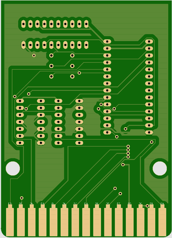
We’ll start with a couple of images which will work as a guide during the assembly.
The first one of them is the component’s layout:

And the second one is the circuit’s scheme. To see it bigger click on the image.

It’s important to realize that, once interface is plugged in Spectrum, components go in the television’s side, remaining the tracks’ side oriented to us. This is done in this way so that the bigger components don’t stumble into Spectrum when connecting interface.
Afterwards, we’ll see that it is shown in the board, but I just warned you that the connector must be soldered in the tracks’ side, but not in the components’ side.
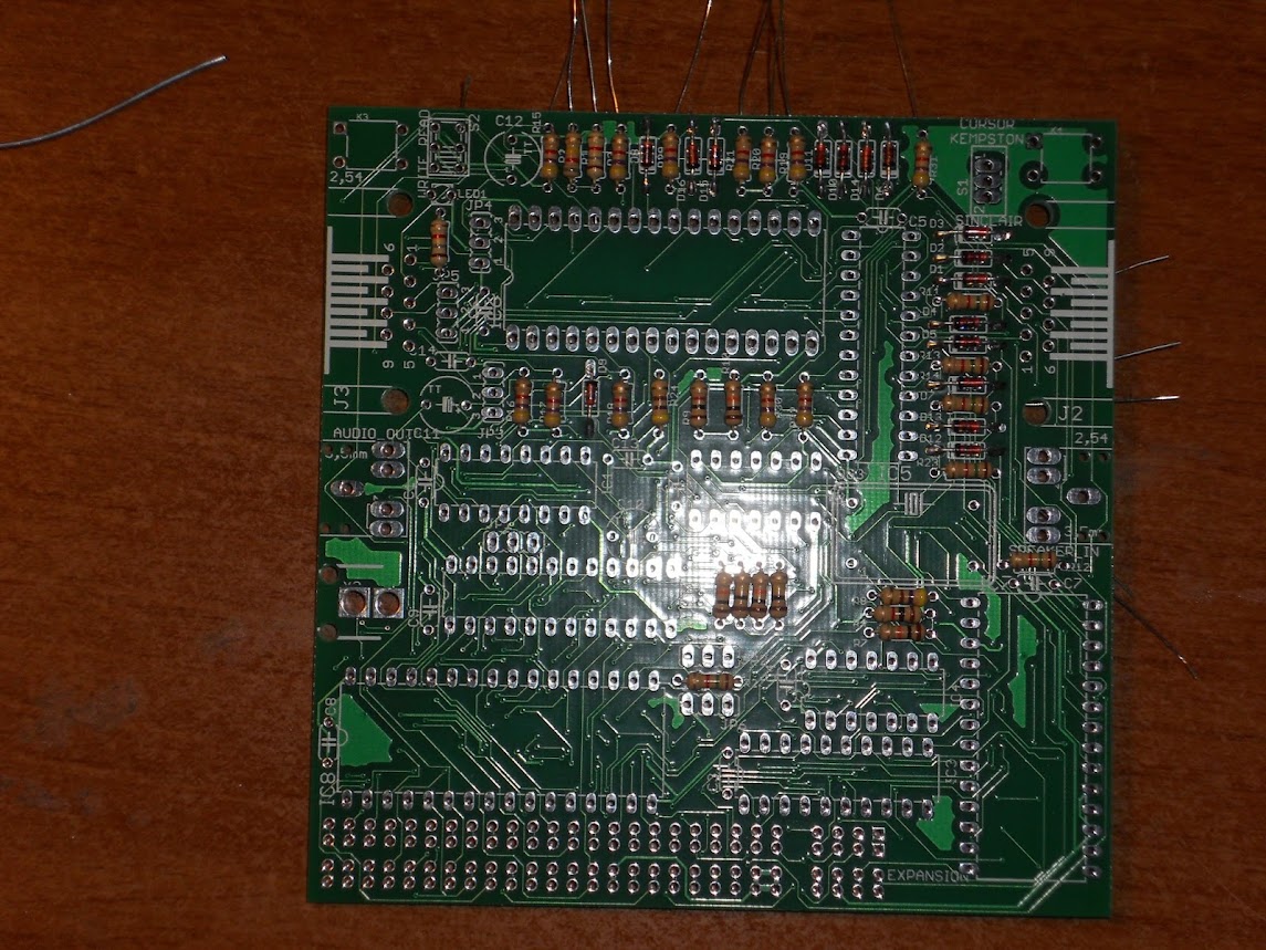
Let’s have a look at the plaque.
Here I show you components’ front.


It’s cool/great, right?
Well, let’s put on our working clothes, heat the soldering iron, take the components and put the tin close to us.
We’ll start soldeing what has the lowest altitude and we’ll end with the highest, so that we’ll be able to put the board on the table without any problem to do welds quietly.
Following that rule, we’ll start with diodes.


Let’s continue with resistors…
Be careful when you reach this point, because, as erratum says, the board has two labeled mistakes.
With that components’ mess , R32 doesn’t have a label and R14 has the label moved, above the diode which is over it.

I tell you I seemed to be pretty smoked cause labels moved from side to side :)
Then we continue with the sockets.

After sockets, we solder the glass, ceramic capacitors and audio connectors.


The two lowest jumpers must be soldered in components’ side, because if we don’t do this they stumble with Spectrum and they don’t let interface be inserted.
Well, it’s my turn to desolder those two jumpers and solder them in the opposite side.
Let’s move on to the EDGE connector and the expansión board.
The design we have has the peculiarity of non copying pin by pin Spectrum’s port with the expansión board, so we can’t solder the expansión board directly with connector EDGE’s welds.
Due to that reason, we have a diferent pad for each thing.
In the board comes a help label that points out in what side and what altitude we have to weld the expasion port or the EDGE connector.
To weld the expansión board we’ll cut two strips of 28 pins and we’ll push the pin number 5 to take it out of the strip. This pin will match later with the Spectrum’s slot’s position.
Once we have strips cut, we take one of them and we insert it where it’s written “expansión” in components’ side.


It’s extremely important to weld this strip before the EDGE connector, since if we don’t do that later we won’t have Access to solder this strip’s pins.
It will look like this:

First we take the corresponding pins to the position number 5 pushing them from below.


Once we’ve soldered the connector we solder the other pins’ strip.


We can just transform this connector in AERIAL.
It must have looked like this:
And it looks like this:
You realized in the previous pictures that this moment is great to solder DB9 connectors for joysticks and insert chips in their BSES/PLINTHS.
When you insert chips in their PLINTHS/BASES we careful with putting the slot in the same position as in the plaque and pay attention because GAL aren’t iterchangeable one another, since each one of them has different functions.
In the packet I sent you they’ll be perfectly labeled as IC10 and IC5 and programed so that it’s EASILY READY.
Let’s weld the expansión plaque nos. To do it we’ll fold slightly those pins we’ve already soldered to make the plaque be fixed in the resulting gap.
Check if the plaque is aligned before welding it.
We move on to soldering the plaque above and below.
After that we just have to put jumpers in the right position and try the invention.
I send you the flash ROM with a TEST set, but if you want to put other different ROMs, you just have to do it with the programmer.
JUMPERS’ POSITION
JP2-With the jumper in position 1-2 interface’s memory is enabled and in position 2-3 Spectrum’s internal memory is enabled.
JP1 and JP6-Their function is to enable the 512kb memory or disable it. With both jumpers in the position 2-3 interface will have 128kb and in the position 1-2 will have 512kb.
JP3 (LOWER bit), JP4 (intermediate bit) and JP5 (SUPERIOR bit)-They’re used to select one of the eight memory flash 64kb blocks. These jumpers in position 2-3 correspond to a 0 and in position 1-2 correspond to 1.
With these three jumpers we create a number of 8 bits which correspond to 64kb block that is active.
INTERNAL RAM’S DISABLING IN OUR 48kb
If we have a 16kb Spectrum we don’t need to touch it when it comes to using our interface, but if it’s a 48kb we’ll need to make a Little internal change in our Spectrum which permits interface to disable THE HIGH MEMORY.
We have two different cases DEPENDING on the plaque’s versión.
For every model from Issue 1 to Issue 4:
To disable the high memory of a -------- we have to put 5v in pin 5 of IC23.
In normal conditions this is achievable BRIDGING/CONNECTING it with pin 14 of the same chip, but in our set up we’ve disabled BUS’ PIN 4ª WHICH WASN’T USED to supply those 5V. Therefore when interface and jumper are inserted in the right position and high memory is disabled automatically, and if you unplug it is enbled again.
We should weld a cable between pin 5 of IC23 and expansion slot’s pin 4ª.
In case our Spectrum is an Issue 5 or 6 we should connect ------35 of IC27 with expansion bus’ 4ª--------------
It isn’t shown in the image because it is under the metallic spendthrift, but it is the ------- which i on 15 place if we start counting from the bottom right side.
ERRATUM
-R32 doesn’t have a sign. It’s the only one that doesn’t have it because it won’t take you a long time to find it. It is the -1k8 resistor which is fixed on the flash memory’s left.
-R14 has a sign displaced upwards, above the D7 diode, that is, it is the resistor located between D7 and D13.
-The video connector is upside-down, ---------------------. This is the biggest mistake and it obligates to make into AERIAL what was supposed to be soldered on plaque. Anyway, we aren’t foolproof.
-JP2 shouldn’t be called DISA17 as it’s written in the plaque, but DISRAM, this is the jumper to disable interface RAM and enable internal one without disconnecting interface.
NECESSARY CORRECTIONS
I’ll expose then necessary corrections so that the circuit works properly.
The first correction is oriented to permit flash memory’s recording and it consists in the addition f a diode that puts at high level chip’s /EO signal when we are trying to write. In the original design 0 it was always put to 0 when we accessed to the chip and this is not right in writing’s case.
The second correction is necessary to add a reset to the GAL which controls paging.
As everyone of that GAL’s--------- were BUSY/FILLED I’ve taken out the utility which disabled the ROM with A14, A15 and MREQ signals.
Lastly, it’s necessary bridging R27 to make external RAM’s disabling work. This isn’t necessary if you don’t need this option.
Finally modifications consist in the addition of 3 diodes (D17, D18 and D19) and a bunch of cables that makes the circuit a Little bit uglier.
Relating to components’ side, changes will look as the following:
If we look at it from tracks’ side, where we have to solder, changes will look like this:
The list of the options we have to realice is the following one:
-Desoldering the D15 anode and soldering a CABLE from the anode to the ------- 4 of IC10.
-Soldering the D17 anode with the D6 anode and the D17 cathode with the D115 cathode.
-Soldering the D18 anode with the ----13 of IC10 and the D18 cathode with the D15 cathode.
-Soldering the D19 anode with the ------------7 of IC10 and the D18 cathode with the D15 cathode.
-Soldering a cable between the ------------14 of IC10 and---------1 of IC3.
-Soldering a cable between both edges of R27.
The IC10 equtions are already modified to add these changes.
POSSIBLE PROBLEMS WE CAN FIND
I’ve noticed that in some Spectrums, when we connect interface the two superior half rows stop working. That is, keys 1234567890.
The problema is provoked by joystick interface.
As you know Sinclair’s protocol and Protek/cursor share the port with superior half rows, translating joystick’s buttons in keys. Well, joystick’s keys which are pressed putt he corresponding bit to 0, whereas the rest is PUT to 1.
This ones are intentionally weak, so if a key in spectrum is pressed this one can put that bit to 0. The way in which that ones’ weakness is forced is with resistors R11, R12, R13, R14, R23 of 1K5.
This 1K5 value is the one which was used in MHT engineers commercial interface and it works in the major part of Spectrums, but I’ve found out with some spectrums that this value is not enough.
I suppose that the problem has to do with the impedance in the membrane, either as a result of being dilapidated or because it has been replaced with another one of higher impedance.
The solution of this problema ( just in case it appears) consists in replacing those resistors with 10K resistors. In the empirical tests that I’ve done this has worked perfectly.
Obviously I can’t try it with every existing spectrum, but in case YOUR joystick didn’t work making this replacement, try it with a lower value, for instance 4K7.
SELECTION ADD-ON BY SOFTWARE
Selection Add-on by software consists basically in replacing JP3, JP4 and JP5 jumpers’ function with a GAL which permits to change the active ROM with the $043B port (1083) with a parcial de-codification (bits A15, A7; A5, A1 and A0).
It’s really important removing jumpers to make the add-on work.
Firstly, the idea was that the add-on just consisted in a GAL with a necessary logic, but fue to the conflicts the divide had with add-on, additional circuitry has been added, which consists basically in a 4 OR DOORS chip (74LS32), three diodes and a 4k7 resistor.
The plaque is supposed to poke on flash memory’s BASE/PLINT, because we have most of the signals we need there. However, there are some signals we have to take from other points of the plaque, such as (A15, /WR, /IORQ, /RESET, /MREQ, BACK_MREQ, BACK_A15).
Let’s start with the plaque’s scheme and we’ll continue then with MAIN PLAQUE’S WIRING.
The methode we’ll use will be putting two rows of 16pins in the inferior part of a prototype’s plaque piece to permit us poke on the flash memory’s base.
In the superior part, slightly displaced ABOVE THE PREVIOUS ONES, we’ll solder other two rows of pins, but SOCKET this time, to work as a base for the flash memory.
We’ll have to weld both EVEN, pin by pi so that we confirm the continuation between flash memory and its original base.
We’ll solder everyone of the pins WITH EACH OTHER (the superior base ones with the inferior pins), one by one except ROMA14 and ROMA15 signals ( -----29 and 3 of the memory) that, as you can see in the scheme they should be separated, because we’ll screen them in the GAL, generating two new ROMA14` , ROMA15` signals.
Here you have a picture of how it should look (sorry for ugly welds =) ):
In the case of ROMA14 (-----29) , and ROMA15 (--3) signals, signals which come from the plaque should be connected to ------- 8 and 9 of the GAL respectively, whereas signals that GO TO the memoery (ROMA14` and ROMA 15`) go to --------18 and 19 of the GAL.
Once we’ve made this, we have the possibility of welding the necessary cables between a narrow base of 24 pins which we’ll solder for the GAL and the new base we`ve improvised for the flash memory.
To do that, we’ll follow the previously shown scheme.
Once we’ve made it, we’ll move on to make the signals’ connections left, with the main plaque.
The scheme that should be followed for those threads is the following one:
To be able to connect and disconnect the plaque I’ve added a Little row of 7 rocket pins which will allow us to connect a plain cable where I’ve soldered pins ------.
I don’t add a picture of how mine looks so as not confuse you, because I have a lot of unnecessary things after lots of tests.
Something you have to take into consideration is that A15 and /MREQ signals, when we add add-on, have to be disconnected of the rear expansionn buus, because add-on’s gal will generate new BACK-A15 and BACK_MREQ signals to connect with the rear expasion bus.
Sorry for the bad picture’s quality, but I haven’t been able to take a better one that close.
The idea is connecting A15 and /MREQ signals with the pins we’ve lifted and BACK_A15 and /BACK_MREQ directly on the expansion bus’ tracks.
I’ve added a piece of thermo-retracting to the cable that goes to the pin, so that they aren’t in contact.
Lastly you’ll have to record the equations in add-on’s gal.
You have here this new GAL’s equations:
COMPONENTS’ LIST
SYSTEM FILES
In the following link, you can download the files you’ll need to programme GAL and flash memory.
You also have schemes and all the VERSION’S SOURCES.
I also attach the main PATCHED ROMs of the +3 to work with superupgrade.
Download
You should take into account that IC10 equations change from versión 0.4, which is the one that corresponds to the plaque. For that reason it’s essential to make modifications in the plaque to make it work.
In the ROMs file you have two different ROMSETs, as well as the BIOS’ sources.
In the case we made the add-on we would be able to take advantage of those ROMSETs characteristics, though, anyway, there are functios we can take advantage of in the case we didn’t make the add-on.
-TEST’S ROMSET. This ROM will permit us to realice the beginning tests to make sure everything works well.
It consists of a starting manu and 31copies of the original Spectrum’s ROM. If we have the add-on connected, when we start up it’ll appear the menú which will permit us select the ROMSET and the ROM we want to start up with.
In the case we didn’t have the add-on we’ll be able to select the acive ROM with jumpers and we’ll press reset.
The ROMs’ beginning message is changed to show us which ROMSET and which ROM is active.
-Example ROMSET. This ROMSET has BIOS installed in the ROM0 ad a series of different systems already copied. If we have the add-on connected we’ll be able to start up the system we want just selecting the corresponding letter to that system and then pressing Enter.
The combination BIOS/add-on doesn’t work well if we don’t have connected the divIDE and it’s likely to come out a new versión with modifiers in the hardware, as well as in the software.
To work with jumpers we should take into consideration that we only have 8 simultaneous systems, although in this case we have complete compatibility with the divide as long as we take into account the following points:
-Each ROM should take 64kb.
-In the case of 32kb ROMs we should copy them twice in the desired SLOT.
-In the case of 16kb ROMs we should make 4 copies.
Games and systems compatible with divide (as Jupiter ACE) will need to disconnect or deactivate it before starting them up.
BIOS’ MANAGEMENT
The main superupgrade’s BIOS’ screen show us a list with the ROMs included in the flash memory.
To start up one of them, we’ll select the corresponding letter and we’ll press “ENTER”.
In in versio 0.2 of the BIOS a tool submenú has been added, which can be accessed pressing “V” and “ENTER”, from the main menu.
In that menu we’ll have tolos to test our interface:
-KEY IN TEST: it’ll show us visually the letters we’re pressing and the three superior bits of each half row.
For the KEY IN we just use bits 0 to 4, whereas bit 6 is used to the EAR input.
To finish the test we’ll press BREAK.
-JOYSTICK’S TEST: it will permit us to make a complete joystick’s test, asking us to press sequentially each one of joystick’s keys. When we get to the Sinclair’s test we should use both joysticks simultaneously.
In the case we press “BREAK” we’ll move on to the next key, though we don’t press the right key.
-RAM’S TEST: it will realize a RAM’s paging test, pointing out how many pages of memoery we have.
It isn’t about a complete RAM’s integrity test, because it just tests the paging.
-AUDIO’S TEST: it will make a musical scale sound for each one of the three AY channels.
-ROM’S PAGE’S SELECTION: This option is thought to those users that don’t insert the add-on.
Remember that the memory is divided in 64kb blocks’ which are selectable with jumpers, and that in each one of the 64kb blocks four 64kb pages fit.
Well, if after starting up the menu we change jumpers to the desired ROM, this option will permit us to select the 16kb page we want to execute.
Once the desired page is selected, the system will ask us to press a key, and then spectrum will be reset executing the programme which is restrained in the selected page.
Alejandro Valero Sebastián (wilco2009)